Phone:86-0714-3056766 E-mail:sukie@hbzpdz.com
Production process of R- flexible PCB
The production of rigid and flexible PCB should be equipped with both FPC and rigid PCB processing equipment. Firstly, electrical engineer layout the circuit and design the shape of the Rigid-flexible PCB according to request. And then, it is delivered to the manufacturer that can produce the of rigid and flexible board. After the DFM process performed by CAM engineer, the production for FPC and rigid PCB can be arranged respectively on corresponding production equipment, then the flexible PCB and rigid PCB are pressed together by pressing machine based on requirement issued by electronic engineers. the rigid and flexible PCB have been finally completed with a series of subsequent process after pressing.Aluminum pcb board
Rigid and flexible PCB design rules and notes
The design of rigid and flexible PCB is much more complicated than the traditional PCB, and there are many points that need attention. In special, the transition zone for rigid and flexible part as well as design related aspects such as circuits, via holes and so on, all of them should follow the requirements of the corresponding design rules.
Via location
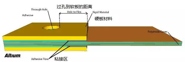
In dynamic use, especially when the flexible PCB need to be bent frequently, via holes should be avoid on flex part as far as possible.Because these holes are easily damaged and cracked. It is allowable to design via holes in the reinforced area of the flex PCB, but via holes along with the edge of stiffener should be avoid. Therefore, a certain of safe distance should be considered when via holes are designed in the combination of rigid and flexible pcb, refer to below picture:
Rules should be followed when design via holes close totransition zone :
50mil shall be ensured between the edge ofholes to the edge of flexible part. a minimum of70mil shall be ensured for high reliability applications.
Mostmanufacturers will not accept distance limits below 30mil.
The same rule applies to via holes designed in flexarea, and this is the most important rule for rigid andflexible PCB design.
Viaholes and pad design
Pad and via holes should be designed as big as possible if it can meet the design requirement, meanwhile the connection between pad and conductor shall apply smooth transition line and avoid right angles. Anchors should be designed for Isolated pads to improve the strengthen of support.
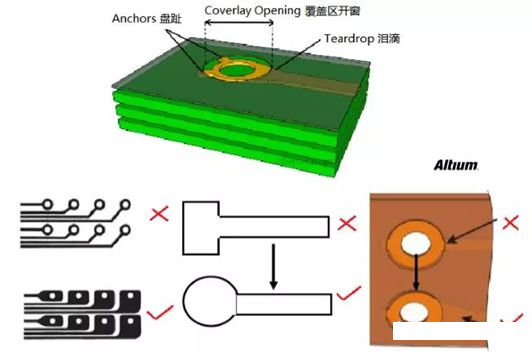
In rigid and flexible PCB production process, via holes or pad could be damaged easily. To lower the risk, the following rule shall be followed in design process:
The bigger the better for pad and annular ring.
Design teardrops the joints between pad and the connecting track for strengthening mechanical support.Aluminum pcb board
Adding anchors to strengthen Reinforcement.
The design of circuits
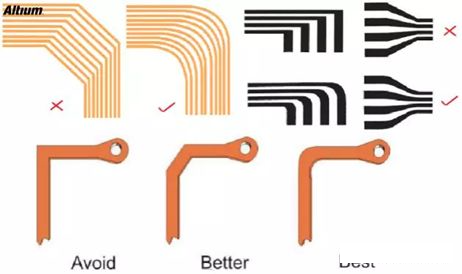
In the flexible Zone, if there are lines in differentlayers. Try to avoid traces on the same route from top and bottom sides, becauseit can cause mechanical damages easily due to uneven force ofthe copper from both sides when bending. Instead, traces should be staggered and crosswise arranged. As below picture shows:Aluminum pcb board
The traces design in the flexible area require a circular arc rather than an angle, contrary to the suggestion of rigid part design. It can protect the traces in flex part and avoid damages. Sudden expansion or contraction of traces should be avoided. Arc and teardrops should be applied on the connection between smaller and bigger traces. Refer to below pictures:
Filling copper for PCB layout design
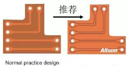
To enhance the flexibility of bending, Copper or ground plane is best to use grid structure. However, for impedance controls and other applications, the electrical characteristics of the grids are not good, So the designer needs to make a reasonable judgment whether grid copper or solid copper should be applied according to design requirements. However, for breakaway frame, solid copper is preferred. Refer to below pictures:
Distance between holes to copper
This distance between holes and copper, we call it as hole copper distance. Flexible material is different from rigid material, so that too closed distance between hole and copper is difficult to deal. Generally, the standard spacing 10mil(min) should be ensured.
For rigid and flexible combination zone, two most important distances must not be ignored.The one is called hole to copper 10mil(min). The other is the Hole to Flex edge mentioned before, which is generally recommended to be 50mil.
Designof R-flex combination zone
In the rigid and flexible combination zone, it is better to design the flexible part in the middle of the stack-up. notes for R-flex combination zone:
The line should be smooth transition and the direction of the line should be perpendicular to the bending direction.
Traces should be evenly distributed throughout the bending area.
PTH should not adopted in rigid and flexible transition zone.

Bending radius in bending zone
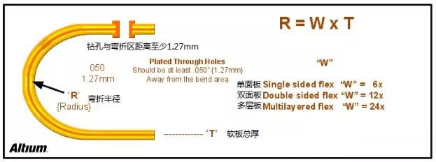
The flexible bending zone of the rigid and flexible board shall be able to withstand 100,000 bending without breaking, short circuit, performance degradation or unacceptable layering. Flexural resistance can be measured by special equipment or by equivalent instrument. In design, bending radius should be followed the relevant requirement. The design of bending radius should be related to the thickness of flexible bending zone and the number of layers. A simple reference standard is R=W x T. T is the total thickness of the flexible board. Single panel W is 6, double panel is 12, multilayer is 24. Therefore, the minimum bending radius of single panel is 6 times thickness, double panel is 12 times, and multilayer is 24 times. They should not be less than 1.6mm.
In one word, thedesign of flexible circuit board is particularly important when perform R-flexPCB design. Flexible PCB design requires the consideration of substrate,bonding layer, copper foil, coverlay . stiffener, surface treatment ofdifferent materials, different thickness, different combinations, and itsperformance, such as peeling strength, flexural resistance, chemical performance, working temperature. In particular, the assembly and application shouldbe considered too. Specific design rules can be referred to IPC standard: IPC-D-249 and IPC-2233.Aluminum pcb board
In addition, with respectto the processing accuracy of flexible PCB. overseas processing accuracy: line width: 50micron; min hole size: 0.1mm;number of layers may more than 10 layers.processingaccuracy in China: line width: 75micron, min hole size: 0.2mm; layer number: 4-6.Designers should know andrefer to above information when perform the R-flex PCB design.